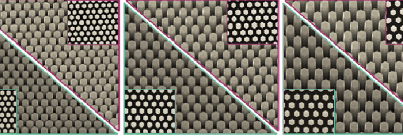
The research line Semiconducting Nanowires & Nanostructures aims at developing and exploring the chemical synthesis of spontaneously grown ZnO nanostructures/nanowires by chemical bath deposition (CBD) and metal-organic chemical vapour deposition (MOCVD). These methods of chemical synthesis can be coupled with technological processes in a cleanroom environment (i.e. lithography, etching, ...) in the framework of the selective area growth of these objects. We are specifically interested in elucidating and monitoring the nucleation and growth mechanisms of nanostructures/nanowires by coupling an experimental approach to a fundamental approach based on thermodynamic simulations. Our activity is also focused on the determination and control of the basic properties of these objects, such as their intrinsic/extrinsic doping (i.e. H, Al, Ga, Cu, ...), their polarity (O and Zn), as well as the effects related to their surfaces. Semiconducting heterostructures based on ZnO nanowires that are bare or combined with direct band gap semiconductors (Sb2S3, SnS, Ga2O3…) are being developed for piezoelectric, optoelectronic (i.e. self-powered UV photodetectors, light emitting diodes), and photovoltaic (i.e. extremely thin absorber solar cells) devices.
Permanent staff
Non permanent staff
Alexandre Dieulesaint (PhD)
Adrien Baillard (PhD)
Emilien Lefebvre (PhD)
Lisa Legardinier (PhD)
Manuel Manrique (PhD)
Andy Séguret (PhD)
Marielena Velasco Enriquez (PhD)
Adrien Baillard (PhD)
Emilien Lefebvre (PhD)
Lisa Legardinier (PhD)
Manuel Manrique (PhD)
Andy Séguret (PhD)
Marielena Velasco Enriquez (PhD)
5 selected publications
[1] R. Parize et al. The Journal of Physical Chemistry C 121, 9672 (2017)
ZnO/TiO2/Sb2S3 Core–Shell Nanowire Heterostructure for Extremely Thin Absorber Solar Cells
[2] T. Cossuet et al. Advanced Functional Materials 28, 1803142 (2018)
ZnO/CuCrO2 Core–Shell Nanowire Heterostructures for Self‐Powered UV Photodetectors with Fast Response
[3] J. Villafuerte et al. The Journal of Physical Chemistry C 124, 16652 (2020)
Zinc Vacancy-Hydrogen Complexes as Major Defects in ZnO Nanowires Grown by Chemical Bath Deposition
[4] Q.C. Bui et al. ACS Applied Materials & Interfaces 12, 29583 (2020)
Morphology Transition of ZnO from Thin Films to Nanowires on Silicon and its Correlated Enhanced Zinc Polarity Uniformity and Piezoelectric Response
[5] C. Lausecker et al. Inorganic Chemistry 60, 1612 (2021)
Chemical Bath Deposition of ZnO Nanowires Using Copper Nitrate as an Additive for Compensating Doping
Review articles
[1] J. Zuniga-Perez et al. Applied Physics Reviews 3, 041303 (2016)
Polarity in GaN and ZnO: Theory, Measurement, Growth, and Devices
[2] V. Consonni et al. Nanotechnology 30, 362001 (2019)
ZnO Nanowires for Solar Cells: A Comprehensive Review
[3] P. Gaffuri et al. Renewable and Sustainable Energy Reviews 143, 110869 (2021)
Potential Substitutes for Critical Materials in White LEDs: Technological Challenges and Market Opportunities
[4] V. Consonni et al. Nano Energy 83, 105789 (2021)
Polarity in ZnO Nanowires: A Critical Issue for Piezotronic and Piezoelectric Devices
Projects
ANR SCENIC (2021-2024, collaborator)
Type: Research National Agency, collaborative program call
Title: Surface charge effects in functionalized GaN and ZnO nanowires: investigation and control
Partnership: IMEP-LaHC (Grenoble), GEEPS (Paris-Saclay), C2N (Paris-Saclay)
ANR IMINEN (2023-2027, coordinator)
Type: Research National Agency, collaborative program call
Title: Elucidating & monitoring nanosized-effects in ZnO nanowires for piezoelectric applications
Partnership: Institut Néel (Grenoble), LTM (Grenoble), LETI (Grenoble), LGEF (Lyon)
ANR ALOFET (2024-2028, collaborator)
Type: Research National Agency, collaborative program call
Title: AlN/Oxide Heterostructures for Polarization Enhanced Transistors
Partnership: Institut Néel (Grenoble), CEA-IRIG-PHELIQS (Grenoble), CEA-IRIG-MEM (Grenoble)
Type: Research National Agency, collaborative program call
Title: Surface charge effects in functionalized GaN and ZnO nanowires: investigation and control
Partnership: IMEP-LaHC (Grenoble), GEEPS (Paris-Saclay), C2N (Paris-Saclay)
ANR IMINEN (2023-2027, coordinator)
Type: Research National Agency, collaborative program call
Title: Elucidating & monitoring nanosized-effects in ZnO nanowires for piezoelectric applications
Partnership: Institut Néel (Grenoble), LTM (Grenoble), LETI (Grenoble), LGEF (Lyon)
ANR ALOFET (2024-2028, collaborator)
Type: Research National Agency, collaborative program call
Title: AlN/Oxide Heterostructures for Polarization Enhanced Transistors
Partnership: Institut Néel (Grenoble), CEA-IRIG-PHELIQS (Grenoble), CEA-IRIG-MEM (Grenoble)
National & international collaborations
- Institut Néel, Grenoble
- LTM, Grenoble
- IMEP-LAHC, Grenoble
- CEA, LETI, Grenoble
- CEA, IRIG, Grenoble
- LEPMI, Grenoble
- SIMaP, Grenoble
- GAEL, Grenoble
- INL, Lyon
- LGEF, Lyon
- CRHEA, Valbonne
- GEEPS, Paris-Saclay
- C2N, Paris-Saclay
- Swansea University, South Wales
- Tallinn University of Technology, Estonia
- Aristotle University of Thessaloniki, Greece
- University of Cambridge, England
- Universitat de Barcelona, Spain