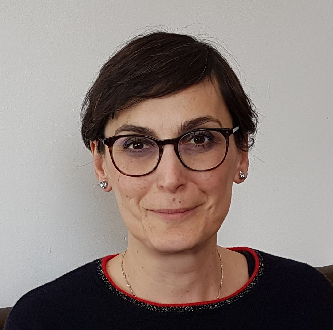
MME SARIGIANNIDOU Eirini
Academic Activities in Grenoble INP - Phelma, UGA
Domaines : Physique et Physique de MatériauxNiveaux : Licence, Master et Formation Continue
Recherche activities
ORCID: 0000-0003-3779-445X
Keywords: Electron Microscopy techniques, Wide band gap Semiconductors, Nitrides, ZnO Nanostructures, Silicon Carbide, Aluminum Silicon Carbides, MBE, Crystal growth, X-ray absorption, MOD, Superconductors, Thermal treatments
Wide band gap Semiconductors studies (III-Nitrides, ZnO, Ga2O3)
Characterization: Use of Transmission Electron Microscopy (TEM) in high resolution, energy filtered, conventional, ASTAR and convergent beam modes to characterize nitrides and ZnO nanostructures (quantum wells, quantum dots and nanowires,…). Quantitative analysis of HRTEM images using the geometric phase analysis, a projection method and images simulations.Epitaxy : Experience in Molecular Beam Epitaxy of III-nitride materials and heterostructures. In situ analytics of growth kinetics by RHEED.
X-ray Absorption spectroscopy (Synchrotron, ESRF): Use of x-ray linear dichroism (XLD) and x-ray magnetic circular dichroism (XMCD) techniques.
Crystal growth and characterization (Carbides, MAX phases)
Structural and Chemical Characterization: Use of electron microscopy techniques (TEM, HAADF, EDS, SEM) to characterize the microstructure, defects and chemical composition of bulk crystals (e.g. SiC, Al4SiC4, Cr2AlC,….)Crystal growth: Experience on PVT growth of Silicon Carbide and Al-Si ternary carbides.
Superconductors
Structural Characterization: Use of TEM techniques to characterize the microstructure of superconducting layers (YBCO) and oxide buffer layers (LZO, CeO2) deposited on LaAlO3 and NiW substrates.Chemical Deposition: Experience on Metal Organic Deposition (MOD) and various annealing treatments used for the growth of oxide buffer layers.
Activités / CV
Nationality: Greek and French
Education
1998-2000: Master in Materials Physics, Aristotle University of Thessaloniki, Greece
2001-2004: PhD in Physics, Joseph Fourier University - Grenoble 1 / CEA-Grenoble / Lab. d’ Etude des Matériaux par Microscopie Avancée (INAC/LEMMA) Subject: Electron Microscopy and Nitride Nanostructures (Superv.: Dr. J.L. Rouviére)
2023: Habilitation à Diriger des Recherches (HDR) "Electron microscopy a key alliance in material science", Ecole Doctorale I‐MEP 2, Grenoble INP -UGA
Professional Experience
Since 2024: Professeurs des universités in Grenoble INP - Phelma, UGA
2006-2024: Associated Professor (MdC) in Grenoble INP - Phelma, UGA
2005 -2006: Post Doctoral studies at CEA-Grenoble / INAC/ NPSC
2004 -2005: Lecturer (ATER) at Joseph Fourier University actual UGA
2000 -2001: Engineer, Aristotle University of Thessaloniki


