Paper by Céline Ternon 2020
The paper "Role played by the nanowire/nanowire junctions in the electrical properties of semiconductor percolating silicon nanowire networks" has been published in Journal of Applied Physics
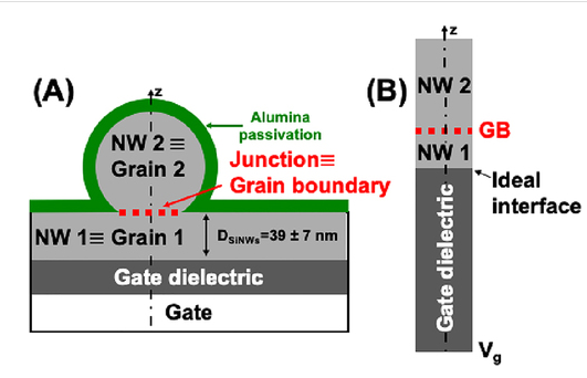
"In this paper, we highlight the key role played by Si nanowire/nanowire junctions in the electrical performance of field-effect transistors (FETs) based on percolating Si nanowire (SiNW) networks, also called nanonets. Using our original technological process to fabricate simultaneously numerous silicon nanonet-based transistors with a variable geometry, we thoroughly investigated in this paper their electrical properties for various channel lengths from 5 to 100 μm. In particular, we evidenced a clear transition in the FET performance, when NW/NW junctions are involved in the conduction path. On the one hand, for channel length shorter than that of nanowires (NWs), the devices are called multiple-parallel-channel FETs as NWs directly bridge the channel, and they exhibit poor electrical performance in terms of OFF current, ON-to-OFF ratio, and subthreshold slope. On the other hand, for channel length longer than that of nanowires (NWs), the devices are called nanonet-FETs (NN-FETs) as the current flows through percolating paths made of NWs and NW/NW junctions and the performance are considerably enhanced. By combining our structural knowledge of the material with experimental observations of electrical properties and modeling results, by relying on the percolation theory, the model for electrical transport in polycrystalline silicon and the principle of potential barrier lowering by the field effect, we propose the junction driven percolation mechanism. It explains the role played by the nanowire/nanowire junctions in the electrical properties of semiconductor percolating nanowire networks and how they drastically enhanced the electrical properties of nanowire-based field-effect transistors despite the disorder introduced by the increasing number of nanowires. As a consequence, by controlling properly the junction interfaces and device geometry for a given NW density, thanks to NW/NW junctions, the NN-based devices are a valuable and promising alternative to improve the electrical performances of NW-based devices for future developments"