Aller au menu Aller au contenu
Synthèse et propriétés de monocristaux, de poudres, films minces ou hétérostructures

Etudes à l'interface avec la matière biologique

> LMGP_ Recherche > Funsurf

Publication de Tabassom Arjmand

Publié le 16 juin 2022
A+Augmenter la taille du texteA-Réduire la taille du texteImprimer le documentEnvoyer cette page par mail cet article Facebook Twitter Linked In
Communiqué du 16 juin 2022 au 31 août 2022

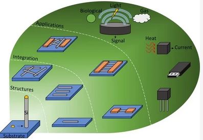
L'article intitulé "Functional Devices from Bottom-Up Silicon Nanowires: A Review" a été publié dans Nanomaterials faisant partie du numéro spéciale "Silica- and Silicon-Based Nanostructures" edité par Céline Ternon

Ici vous trouverez l'article de Tabassom. Et ici l'éditorial de Céline Ternon pour le numéro spéciale
"This paper summarizes some of the essential aspects for the fabrication of functional devices from bottom-up silicon nanowires. In a first part, the different ways of exploiting nanowires in functional devices, from single nanowires to large assemblies of nanowires such as nanonets (two-dimensional arrays of randomly oriented nanowires), are briefly reviewed. Subsequently, the main properties of nanowires are discussed followed by those of nanonets that benefit from the large numbers of nanowires involved. After describing the main techniques used for the growth of nanowires, in the context of functional device fabrication, the different techniques used for nanowire manipulation are largely presented as they constitute one of the first fundamental steps that allows the nanowire positioning necessary to start the integration process. The advantages and disadvantages of each of these manipulation techniques are discussed. Then, the main families of nanowire-based transistors are presented; their most common integration routes and the electrical performance of the resulting devices are also presented and compared in order to highlight the relevance of these different geometries. Because they can be bottlenecks, the key technological elements necessary for the integration of silicon nanowires are detailed: the sintering technique, the importance of surface and interface engineering, and the key role of silicidation for good device performance. Finally the main application areas for these silicon nanowire devices are reviewed."
A+Augmenter la taille du texteA-Réduire la taille du texteImprimer le documentEnvoyer cette page par mail cet article Facebook Twitter Linked In

mise à jour le 17 juin 2022

  • Tutelle CNRS
  • Tutelle Grenoble INP
Université Grenoble Alpes