Publication de Sven Tengeler 2017
Le papier "(001) 3C SiC/Ni contact interface: In situ XPS observation of annealing induced Ni2Si formation and the resulting barrier height changes" a été publié dans Applied Surface Science

Ici vous trouverez le papier de Sven Tengeler
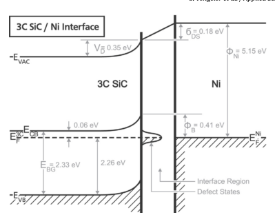
"The electronic states of the (001) 3C SiC/Ni interface prior and post annealing are investigated via an in situ XPS interface experiment, allowing direct observation of the induced band bending and the transformation from Schottky to ohmic behaviour for the first time. A single domain (001) 3C SiC sample was prepared via wet chemical etching. Nickel was deposited on the sample in multiple in situ deposition steps via RF sputtering, allowing observation of the 3C SiC/Ni interface formation. Over the course of the experiments, an upward band bending of 0.35 eV was observed, along with defect induced Fermi level pinning. This indicates a Schottky type contact behaviour with a barrier height of 0.41 eV. The subsequent annealing at 850 °C for 5 min resulted in the formation of a Ni2Si layer and a reversal of the band bending to 0.06 eV downward. Thus explaining the ohmic contact behaviour frequently reported for annealed n-type 3C SiC/Ni contacts."