L'article intitulé "Selective spatial atomic layer deposition of Cu, Cu2O, and CuO thin films in the open air: reality or fiction?" a été publié dans Materials Today Chemistry
au
Ici vous trouverez l'article d' A Sekkat
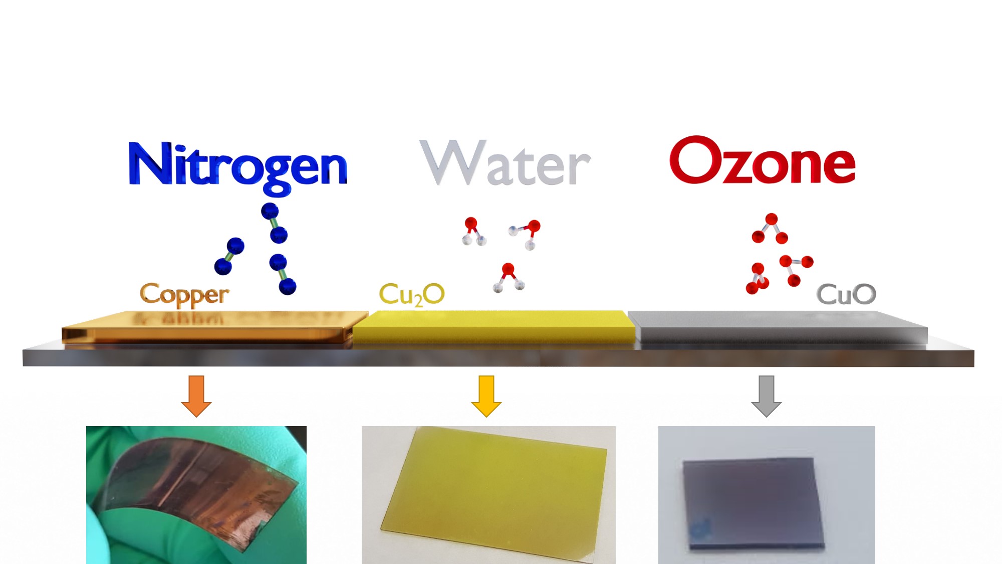
"Copper and binary copper oxide thin films are key materials for microelectronic, optoelectronic, and sensing devices. Herein, we report innovative atmospheric pressure spatial atomic layer deposition processes enabling the facile control over the copper oxidation state. The selective deposition of Cu, Cu2O, and CuO thin films at low temperatures (160–260 °C) has been achieved by using Cu(I)(hfac)(tmvs) as copper source and nitrogen, water, or ozone as coreactants, respectively. The three obtained materials are pure and crystalline, as revealed by X-ray absorption spectroscopy, X-ray photoelectron spectroscopy, and X-ray diffraction. The deposition mechanism of the Cu, Cu2O, and CuO phases is based on disproportionation, hydrolysis, and oxidation reactions. Interestingly, metallic copper films with resistivity as low as ∼3.7 × 10⁻⁶ Ω·cm have been obtained, and resistivity values of 100 Ω·cm and 0.2 Ω·cm have been measured for the Cu2O and CuO semiconductor layers, respectively. Although working in an open-air environment, the oxidation state of copper-based thin films can be controlled using the same precursor, thus reducing cross-contamination and allowing for a faster and more reliable process. This demonstrates the versatility of atmospheric-pressure spatial atomic layer deposition and opens prospects for the manufacturing of novel devices such as wearables, sensors, or flexible electronics."