Papier de Maxime Legallais
Le papier "Wafer-scale HfO2 encapsulated silicon nanowire field effect transistor for efficient label-free DNA hybridization detection in dry environment a été publié dans Nanotechnology
Ici vous trouverez le papier de Maxime Legallais
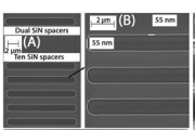
" Silicon nanowire (SiNW) charge based biosensors are attractive for DNA sensing applications due to their compactness and large surface-to-volume ratio. Small feature size, low production cost, repeatability, high sensitivity and selectivity are some of the key requirements for biosensors. The most common e-beam manufacturing method employed to manufacture sub-nm SiNWs is both cost and time intensive. Therefore, we propose a highly reproducible CMOS industry grade low-cost process to fabricate SiNW based field effect transistors on 4"-wafers. The 60 nm wide SiNWs reported in this paper are fabricated using the sidewall transfer lithography process which is a self-aligned-double-patterning I-line lithography process that also facilitates encapsulation of the SiNW surface with a thin HfO<sub>2</sub> layer on which DNA probes are grafted to finalize the biosensors. Upon DNA hybridization, SiNW devices exhibit threshold voltage shift larger than the noise introduced by the exposition to saline solutions used for the bioprocesses. More specifically, based on a statistical analysis, we demonstrate that 85% of the tested devices exhibit a positive threshold voltage shift after DNA hybridization. These promising results make way for the monolithic integration of SiNW biosensors and CMOS circuitry to realize a point of care device which can offer reliable real time electrical readout. "