Paper by Olfa KARKER 2021
The paper "Optimizing interferences of DUV lithography on SOI substrates for the rapid fabrication of sub-wavelength features" has been published in Nanotechnology
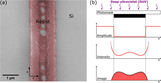
"Scalable fabrication of Si nanowires with a critical dimension of about 100 nm is essential to a variety of applications. Current techniques used to reach these dimensions often involve e-beam lithography or deep-UV (DUV) lithography combined with resolution enhancement techniques. In this study, we report the fabrication of <150 nm Si nanowires from SOI substrates using DUV lithography (λ = 248 nm) by adjusting the exposure dose. Irregular resist profiles generated by in-plane interference under masking patterns of width 800 nm were optimized to split the resulting features into twin Si nanowires. However, masking patterns of micrometre size or more on the same photomask does not generate split features. The resulting resist profiles are verified by optical lithography computer simulation based on Huygens−Fresnel diffraction theory. Photolithography simulation results validate that the key factors in the fabrication of subwavelength nanostructures are the air gap value and the photoresist thickness. This enables the parallel top-down fabrication of Si nanowires and nanoribbons in a single DUV lithography step as a rapid and inexpensive alternative to conventional e-beam techniques."