-
- au
Ici vous trouverez le papier de D. Muñoz-Rojas
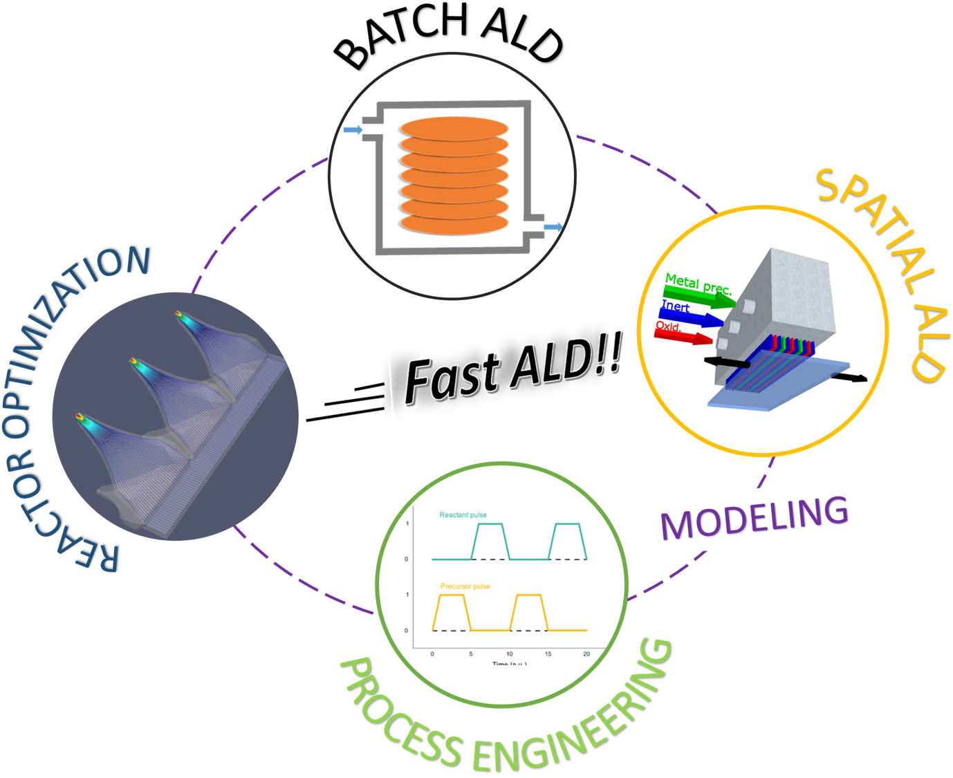
"Atomic layer deposition (ALD) has been traditionally regarded as an extremely powerful but slow thin-film deposition technique. The (perceived) limitation in terms of deposition rate has resulted in a slow penetration of the technology into mass manufacturing beyond established applications in the semiconductor industry until recently. At present, several developments have resulted in a significant increase in the use of ALD in a number of mass manufacturing applications. On the one hand, there is an increasing demand from the device makers side to incorporate nanotechnology in their products that relies on the unique advantages of ALD. On the other hand, a number of technical improvements have been implemented in the ALD method allowing it to be much faster. In this article, we provide an overview of different high-throughput (HT) ALD approaches, putting them in perspective with other common HT deposition techniques already used in the industry. As an example, the use of HT ALD for the encapsulation of organic light-emitting diode is discussed."


